- 您现在的位置:买卖IC网 > Sheet目录312 > AT25DF321-SU (Atmel)IC FLASH 32MBIT 70MHZ 8SOIC
�� �
�
�?� Write� Disable� operation� completes� successfully�
�?� Write� Status� Register� operation� completes� successfully� or� aborts�
�?� Protect� Sector� operation� completes� successfully� or� aborts�
�?� Unprotect� Sector� operation� completes� successfully� or� aborts�
�?� Byte/Page� Program� operation� completes� successfully� or� aborts�
�?� Block� Erase� operation� completes� successfully� or� aborts�
�?� Chip� Erase� operation� completes� successfully� or� aborts�
�If� the� WEL� bit� is� in� the� logical� “1”� state,� it� will� not� be� reset� to� a� logical� “0”� if� an� operation� aborts�
�due� to� an� incomplete� or� unrecognized� opcode� being� clocked� into� the� device� before� the� CS� pin� is�
�deasserted.� In� order� for� the� WEL� bit� to� be� reset� when� an� operation� aborts� prematurely,� the� entire�
�opcode� for� a� program,� erase,� Protect� Sector,� Unprotect� Sector,� or� Write� Status� Register� com-�
�mand� must� have� been� clocked� into� the� device.�
�10.1.6�
�RDY/BSY� Bit�
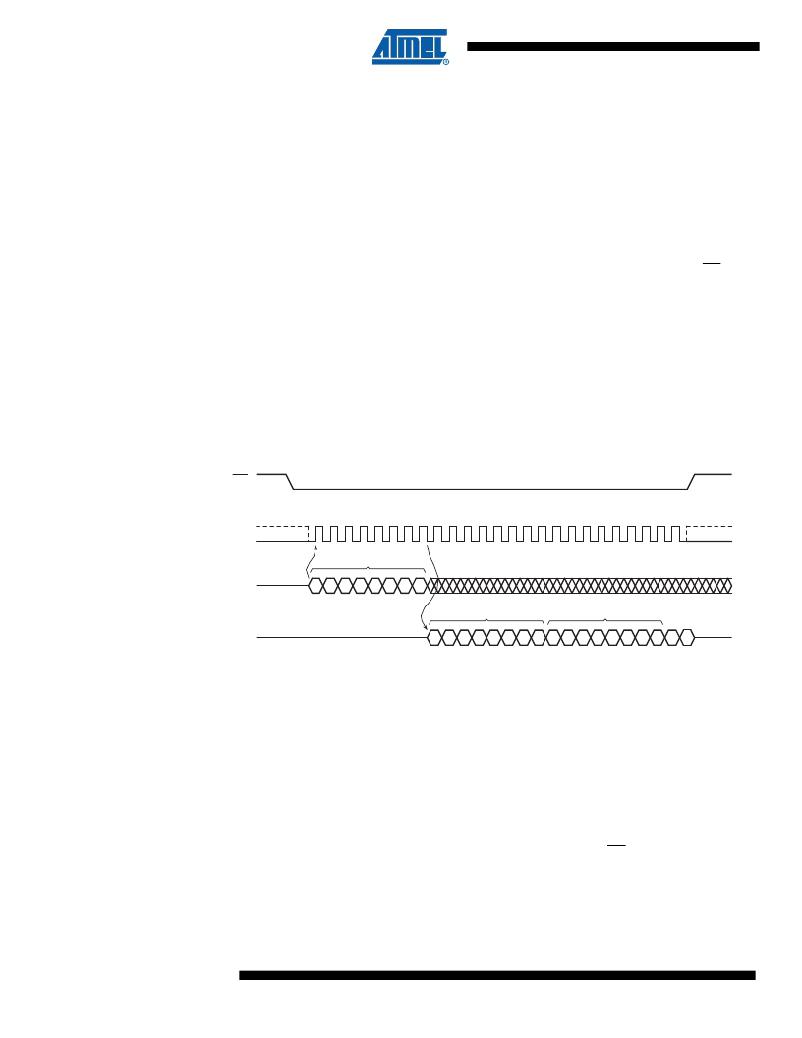
�The� RDY/BSY� bit� is� used� to� determine� whether� or� not� an� internal� operation,� such� as� a� program�
�or� erase,� is� in� progress.� To� poll� the� RDY/BSY� bit� to� detect� the� completion� of� a� program� or� erase�
�cycle,� new� Status� Register� data� must� be� continually� clocked� out� of� the� device� until� the� state� of�
�the� RDY/BSY� bit� changes� from� a� logical� “1”� to� a� logical� “0”.�
�Figure� 10-1.� Read� Status� Register�
�CS�
�0�
�1�
�2�
�3�
�4�
�5�
�6�
�7�
�8�
�9�
�10� 11� 12� 13� 14� 15� 16� 17� 18� 19� 20� 21� 22� 23� 24�
�SCK�
�OPCODE�
�SI�
�0�
�0�
�0�
�0�
�0�
�1�
�0�
�1�
�MSB�
�STATUS� REGISTER� DATA�
�STATUS� REGISTER� DATA�
�SO�
�HIGH-IMPEDANCE�
�D�
�D�
�D�
�D�
�D�
�D�
�D�
�D�
�D�
�D�
�D�
�D�
�D�
�D�
�D�
�D�
�D�
�D�
�10.2�
�Write� Status� Register�
�MSB�
�MSB�
�MSB�
�The� Write� Status� Register� command� is� used� to� modify� the� SPRL� bit� of� the� Status� Register�
�and/or� to� perform� a� Global� Protect� or� Global� Unprotect� operation.� Before� the� Write� Status� Regis-�
�ter� command� can� be� issued,� the� Write� Enable� command� must� have� been� previously� issued� to�
�set� the� WEL� bit� in� the� Status� Register� to� a� logical� “1”.�
�To� issue� the� Write� Status� Register� command,� the� CS� pin� must� first� be� asserted� and� the� opcode�
�of� 01h� must� be� clocked� into� the� device� followed� by� one� byte� of� data.� The� one� byte� of� data� con-�
�sists� of� the� SPRL� bit� value,� a� don't� care� bit,� four� data� bits� to� denote� whether� a� Global� Protect� or�
�Unprotect� should� be� performed,� and� two� additional� don’t� care� bits� (see� Table� 10-2� ).� Any� addi-�
�tional� data� bytes� that� are� sent� to� the� device� will� be� ignored.� When� the� CS� pin� is� deasserted,� the�
�SPRL� bit� in� the� Status� Register� will� be� modified� and� the� WEL� bit� in� the� Status� Register� will� be�
�reset� back� to� a� logical� “0”.� The� values� of� bits� 5,� 4,� 3,� and� 2� and� the� state� of� the� SPRL� bit� before�
�the� Write� Status� Register� command� was� executed� (the� prior� state� of� the� SPRL� bit)� will� determine�
�whether� or� not� a� Global� Protect� or� Global� Unprotect� will� be� perfomed.� Please� refer� to� the� “Global�
�Protect/Unprotect”� section� on� page� 15� for� more� details.�
�22�
�AT25DF321�
�3669B–DFLASH–6/09�
�发布紧急采购,3分钟左右您将得到回复。
相关PDF资料
AT25F1024AN-10SU-2.7
IC FLASH 1MBIT 33MHZ 8SOIC
AT25F2048N-10SU-2.7
IC FLASH 2MBIT 33MHZ 8SOIC
AT25F4096W-10SU-2.7
IC FLASH 4MBIT 33MHZ 8SOIC
AT25HP512W2-10SI-2.7 SL383
IC EEPROM 512KBIT 10MHZ 16SOIC
AT26DF081A-SSU
IC FLASH 8MBIT 70MHZ 8SOIC
AT26DF161-SU
IC FLASH 16MBIT 66MHZ 8SOIC
AT26DF161A-MU
IC FLASH 16MBIT 70MHZ 8QFN
AT26DF321-SU
IC FLASH 32MBIT 66MHZ 8SOIC
相关代理商/技术参数
AT25DF512C-MAHNGU-T
功能描述:IC FLASH 512KB 8UDFN 制造商:adesto technologies 系列:- 包装:带卷(TR) 零件状态:有效 格式 - 存储器:闪存 存储器类型:FLASH 存储容量:512K(64K x 8) 速度:85MHz 接口:SPI 串行 电压 - 电源:1.65 V ~ 3.6 V 工作温度:-40°C ~ 85°C(TC) 封装/外壳:8-UFDFN 裸露焊盘 供应商器件封装:8-UDFN(2x3) 标准包装:5,000
AT25DF512C-MAHNGU-Y
功能描述:IC FLASH 512KB 8UDFN 制造商:adesto technologies 系列:- 包装:托盘 零件状态:停产 格式 - 存储器:闪存 存储器类型:FLASH 存储容量:512K(64K x 8) 速度:85MHz 接口:SPI 串行 电压 - 电源:1.65 V ~ 3.6 V 工作温度:-40°C ~ 85°C(TC) 封装/外壳:8-UFDFN 裸露焊盘 供应商器件封装:8-UDFN(2x3) 标准包装:490
AT25DF512C-MAHN-T
功能描述:IC FLASH 512KB 8UDFN 制造商:adesto technologies 系列:- 包装:剪切带(CT) 零件状态:有效 格式 - 存储器:闪存 存储器类型:FLASH 存储容量:512K(64K x 8) 速度:85MHz 接口:SPI 串行 电压 - 电源:1.65 V ~ 3.6 V 工作温度:-40°C ~ 85°C(TC) 封装/外壳:8-UFDFN 裸露焊盘 供应商器件封装:8-UDFN(2x3) 标准包装:1
AT25DF512C-MAHN-Y
功能描述:IC FLASH 512KB 8UDFN 制造商:adesto technologies 系列:- 包装:托盘 零件状态:停产 格式 - 存储器:闪存 存储器类型:FLASH 存储容量:512K(64K x 8) 速度:85MHz 接口:SPI 串行 电压 - 电源:1.65 V ~ 3.6 V 工作温度:-40°C ~ 85°C(TC) 封装/外壳:8-UFDFN 裸露焊盘 供应商器件封装:8-UDFN(2x3) 标准包装:490
AT25DF512C-SSHN-B
功能描述:IC FLASH 512KB 8SOIC 制造商:adesto technologies 系列:- 包装:管件 零件状态:有效 格式 - 存储器:闪存 存储器类型:FLASH 存储容量:512K(64K x 8) 速度:85MHz 接口:SPI 串行 电压 - 电源:1.65 V ~ 3.6 V 工作温度:-40°C ~ 85°C(TC) 封装/外壳:8-SOIC(0.154",3.90mm 宽) 供应商器件封装:8-SOIC 标准包装:98
AT25DF512C-SSHNGU-B
功能描述:IC FLASH 512KB 8SOIC 制造商:adesto technologies 系列:- 包装:管件 零件状态:有效 格式 - 存储器:闪存 存储器类型:FLASH 存储容量:512K(64K x 8) 速度:85MHz 接口:SPI 串行 电压 - 电源:1.65 V ~ 3.6 V 工作温度:-40°C ~ 85°C(TC) 封装/外壳:8-SOIC(0.154",3.90mm 宽) 供应商器件封装:8-SOIC 标准包装:98
AT25DF512C-SSHNGU-T
功能描述:IC FLASH 512KB 8SOIC 制造商:adesto technologies 系列:- 包装:带卷(TR) 零件状态:有效 格式 - 存储器:闪存 存储器类型:FLASH 存储容量:512K(64K x 8) 速度:85MHz 接口:SPI 串行 电压 - 电源:1.65 V ~ 3.6 V 工作温度:-40°C ~ 85°C(TC) 封装/外壳:8-SOIC(0.154",3.90mm 宽) 供应商器件封装:8-SOIC 标准包装:4,000
AT25DF512C-SSHN-T
功能描述:IC FLASH 512KB 8SOIC 制造商:adesto technologies 系列:- 包装:剪切带(CT) 零件状态:停产 格式 - 存储器:闪存 存储器类型:FLASH 存储容量:512K(64K x 8) 速度:85MHz 接口:SPI 串行 电压 - 电源:1.65 V ~ 3.6 V 工作温度:-40°C ~ 85°C(TC) 封装/外壳:8-SOIC(0.154",3.90mm 宽) 供应商器件封装:8-SOIC 标准包装:1